Nanolayers for germanium surface passivation prepared by Atomic Layer Deposition and Chemical Vapor Deposition
Willem-Jan Berghuis defended his PhD thesis at the department of Applied Physics and Science Education on October 25th.

Smartphones, laptops, and the internet that connects them are truly indispensable to our modern way of living. At the heart of these technologies are silicon-based chips. The continuous desire for improvement is however pushing silicon (Si) to its limits. Germanium (Ge) seems a promising semiconductor to complement Si and overcome some of its deficiencies. Successful implementation of Ge involves many challenges including the electronic losses at its surface. In this context Willem-Jan Berghuis, researcher in the Plasma & Materials Processing group, investigated the passivation of Ge surfaces by ultrathin films deposited by state-of-the-art deposition techniques such as ALD.

Promises of germanium
Faster internet, faster computer chips, and new chip functionalities can be enabled by using light as information carrier instead of electricity. Essential to this are nanoscale lasers and detectors that can transform light signals to electrical signal and vice versa. Silicon is generally not suited for these nano-lasers and nano-detectors since it cannot efficiently emit and absorb light. Germanium and silicon-germanium are however materials that can have this ability. This ability can be achieved by for example alloying them with tin or by growing them in a special crystal structure. The latter is an award-winning approach that is currently pioneered at the Advanced Nanomaterials & Devices research group of TU/e. Ge-based materials are particularly promising for high volume production since they are relatively well compatible with existing silicon chip technology and the existing infrastructure. Read more on this in the article 'Light from silicon proclaimed as Breakthrough of the Year’.
Low recombination losses
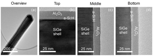
Management of losses in nanoscale lasers and detectors is important to make the technology successful. One of the losses takes place at the germanium surface, the place where Ge meets other layers in the chip. Defects at the surface facilitate a detrimental recombination current: the device works less efficient and it creates heat. In his PhD research, Berghuis investigated ultrathin layers of material to reduce these surface losses. The layers are only tens or hundreds of atoms thick and are synthesized in the cleanroom of the TU/e by high-tech techniques such as Atomic Layer Deposition (ALD). Especially effective proved a thin interlayer of amorphous silicon in combination with atomic-layer-deposited aluminum oxide film. This strategy leads to very low recombination losses. Key to the success was the cleaning of the surface prior to the deposition as well as the presence of a very high density of fixed electric charges in this material stack. Several other materials have been investigated as well, which has resulted in a toolbox of films and strategies to reduce the recombination losses at the Ge surface. Additionally, the understanding of the topic has improved substantially.
Energy efficient
The results are useful to improve the efficiency of germanium-based devices such as nanolasers, photodetectors, solar cells, and even future generation transistors. This ultimately can contribute to a future with internet and electronic devices that work faster and more energy efficient. Additionally, it can provide a contribution to making new medical diagnosis devices and technologies like self-driving cars and broadly available.
Title of PhD thesis: ‘Nanolayers for germanium surface passivation prepared by Atomic Layer Deposition and Chemical Vapor Deposition'.
Supervisors: Erwin Kessels and Bart Macco.