Passivation of semiconductors with nanolayers
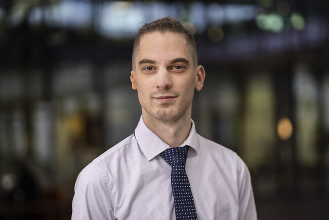
Roel Theeuwes defended his PhD thesis at the Department of Applied Physics and Science Education on November 17th.
Semiconductors materials drive many of the technologies that we use every day, such as computers, displays, LEDs, and solar cells. In these devices, the surfaces and interfaces of the semiconductors can suffer from defects, which severely limit device performance. To make technologies faster, smaller, cheaper, and more efficient, it is crucial that these defects are minimized, which can be accomplished using surface passivation of the semiconductors. For his PhD research, Roel Theeuwes looked at use of nanolayers to passivate semiconductor surfaces.
In semiconductor manufacturing, passivation is a treatment used to make semiconductors passive in nature. In other words, if a semiconductor surface doesn’t respond to or interact with its surroundings, it is less likely to suffer damage via erosion, for example.
To effectively passivate the surface of a semiconductor, multiple steps are typically required. First, the surface is cleaned and surface layers are removed. Second, passivating nanolayers are applied on the semiconductor surface (approximately 10-100 nm thick, about 4-40 times the width of a DNA molecule). Finally, a high temperature treatment (300 to 800 °C) is then applied.
Magic
It is during the second step of this process where the magic happens, with a number of passivating nanolayer options already available.
However, novel nanolayer stacks with unique properties may provide opportunities to further improve semiconductor surface passivation processes. These nanolayer stacks can be synthesized with atomic level accuracy, using so-called atomic scale processing methods.
Nanolayer stacks
For his PhD research, Roel Theeuwes examined the novel nanolayer stacks of phosphorus oxide and aluminum oxide (POx/Al2O3) and p+ doped-poly silicon and aluminum oxide (p+ poly-Si/Al2O3). These stacks show great promise for use in current and next-generation silicon solar cells, but can also be utilized in many other applications.
The POx/Al2O3 stacks enable state-of-the-art surface passivation of textured n+ doped silicon, which is used on the front surface of industrial silicon solar cells. This excellent passivation is enabled by a unique combination of an extremely low number of defects at the interface, and a large number of trapped positive charges.
This combination has so far not been achieved using any other nanolayers. These POx/Al2O3 stacks similarly lead to excellent surface passivation of germanium, which is a semiconductor used for example in computers and infrared optics. Application of POx/Al2O3 also led to the removal of the surface layers of germanium, which can potentially allow for simplified device fabrication workflows, as the first two steps of the surface passivation may be combined.
Solar cells
The p+ poly-Si/Al2O3 stacks can be used in next-generation silicon solar cells. The role of the Al2O3 nanolayer in improving the surface passivation has been further clarified. It turns out that good surface passivation can be achieved regardless of the atomic layer deposition (ALD) method used to synthesize the Al2O3 layer, which provides freedom in process design.
However, the behavior of hydrogen, which is an important agent in achieving excellent surface passivation on silicon, is found to be affected by both the different ALD Al2O3 nanolayers as well as the p+ poly-Si. The additional insights gained may aid the integration of p+ poly-Si/Al2O3 stacks in next-generation solar cells.
Together, these investigations have improved the understanding of these nanolayer stacks for semiconductor surface passivation and have shown that excellent surface passivation of various semiconductor materials can be achieved.
This extended the toolbox for semiconductor surface passivation, which can benefit a wide variety of electronic and photonic devices.
Title of PhD thesis: Semiconductor Surface Passivation: Nanolayer Stacks by Atomic Scale Processing. Supervisors: Erwin Kessels and Bart Macco.
Media contact
Latest news