Research Profile
Nanophotonics with Layered Semiconductor
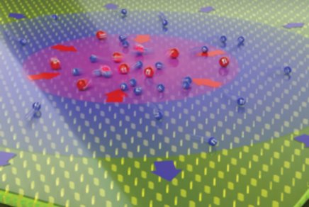
Electrons in two-dimensional layered semiconductors like MoS2 possess additional degrees of freedom compared to conventional semiconductors. Apart from charge and spin, they can be assigned valley (direction) and layer indexes. The opens up many opportunities for the observation of novel physical phenomena and constitutes a new resource for the design of optoelectronic devices for information processing.
The interplay between spin, valley and layer numbers in few-layer van der Waals semiconductors gives rise to very rich exciton Physics. Our team investigates the optical properties of these fascinating materials through a combination of low-temperature photoluminescence, optical polarization, magneto-photoluminescence, and photocurrent techniques.
Chiral Nano-Optics
An overarching goal of our research is a better understanding and exploitation of optical chirality at the nanoscale: its physical origin, its enhancement and manipulation, and possible chiral nanophotonic devices. A major focus of our research is thus the demonstration of novel nano-optical effects governed by specific spin and valley Physics.
News


Recent Publications
Our most recent peer reviewed publications
-
Ershad Mohammadi,T.V. Raziman,Alberto G. Curto
Nanophotonic Chirality Transfer to Dielectric Mie Resonators
Nano Letters (2023) -
Rasmus H. Godiksen,Shaojun Wang,T.V. Raziman,Jaime Gómez Rivas,Alberto G. Curto
Impact of indirect transitions on valley polarization in WS2 and WSe2
Nanoscale (2022) -
Stan E.T. ter Huurne,Adonai Rodrigues Da Cruz,Niels van Hoof,Rasmus H. Godiksen,Sara A. Elrafei,Alberto G. Curto,Michael E. Flatté,Jaime Gómez Rivas
High-Frequency Sheet Conductance of Nanolayered WS2Crystals for Two-Dimensional Nanodevices
ACS Applied Nano Materials (2022) -
T.V. Raziman,Shaojun Wang,Jaime Gómez Rivas,Alberto G. Curto
Exciton Diffusion and Annihilation in Nanophotonic Purcell Landscapes
Advanced Optical Materials (2022) -
T.V. Raziman,Shaojun Wang,Jaime Gómez Rivas,Alberto G. Curto
Exciton Diffusion and Annihilation in Nanophotonic Purcell Landscapes
Advanced Optical Materials (2022)
Contact
-
Visiting address
bc. Philip RamcharanFluxGroene Loper 195612 AP EindhovenNetherlands -
Postal address
Lukas Amalradadr.h.c. Jack HassanDemirboulevard1121JC DongenNetherlands -
Postal address
drs Luuk Elsjan of Wipper ADDepartment of Applied PhysicsP.O. Box 135600 MB EindhovenNetherlands -
TeamleadWessel Visser MÇakirdreef2631VK Vlijmen

